ABOUT US
Laser fabrication is a precise method for controllable material removal via laser radiation. “Light Density” provides high-tech laser micro-fabrication solutions and service. During years of implementing various industrial and scientific projects our team has gained beneficial expertise and know-how knowledge in the laser material processing field. Our main field of expertise includes precise laser milling, cutting, scribing, deep engraving, drilling, surface structuring and modification of various materials (glass, sapphire, metals, semiconductors, ceramics, polymers, composites and etc.).
OUR SERVICES
COMPETENCES
Laser based rear side glass processing can offer high quality and throughput, which can be used for glass drilling, cutting and milling applications. The laser cuts are taper – less, therefore extremely high aspect ratio features can be fabricated. Laser based processing can maintain high throughput with highest processing quality keeping surface chipping bellow 100 µm.
Materials: soda lime (SLG), borosilicate glass, fused silica;
Quality: Surface chipping <100 µm, sidewall roughness <2 µm;
Cutting throughput: 0.6 m/min (1 mm SLG glass), 0.12 m/min (5 mm SLG glass), accuracy ±50 µm;

One of the most material-efficient and energy-efficient glass cutting techniques is to locally weaken the material along the cutting path by generating cracks or material modifications and then separate sheets by applying thermal or mechanical load. We demonstrate the possibility to cut glasses up to 5 mm thickness by applying laser induced modifications. The cutting process can offer high cutting efficiency, were 1 mm thick glass sheet can be cut with speed of 240 mm/s.

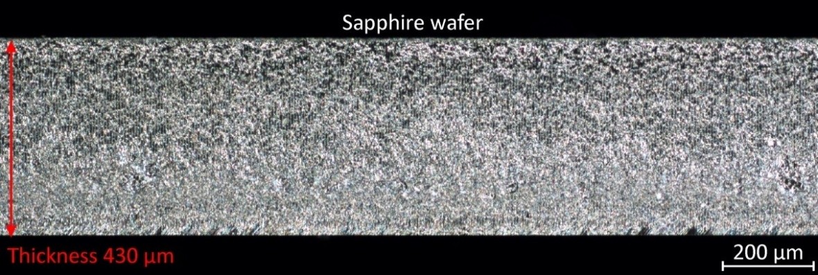
We introduce new effective method for efficient dicing of sapphire wafers by combined dual-wavelength double-pulse laser irradiation. The new innovative effect allowed utilisation of laser energy up to four times more efficiently for internal modification initiation in sapphire. This method opens new opportunities for manufacturers of the GaN-based light-emitting diodes by fast and precise separation of sapphire substrates.

Deep 3D laser engraving technology can be applied for various materials processing. The use of picosecond laser pulses for processing ensures high processing quality and speed. Burr and melt formation are significantly reduced compared to conventional nanosecond laser processing.
Materials: metals, semiconductors, ceramics, glass, polymers.
Ablation precision: 50 μm.
Ablation rate: 6 mm3/min (copper)

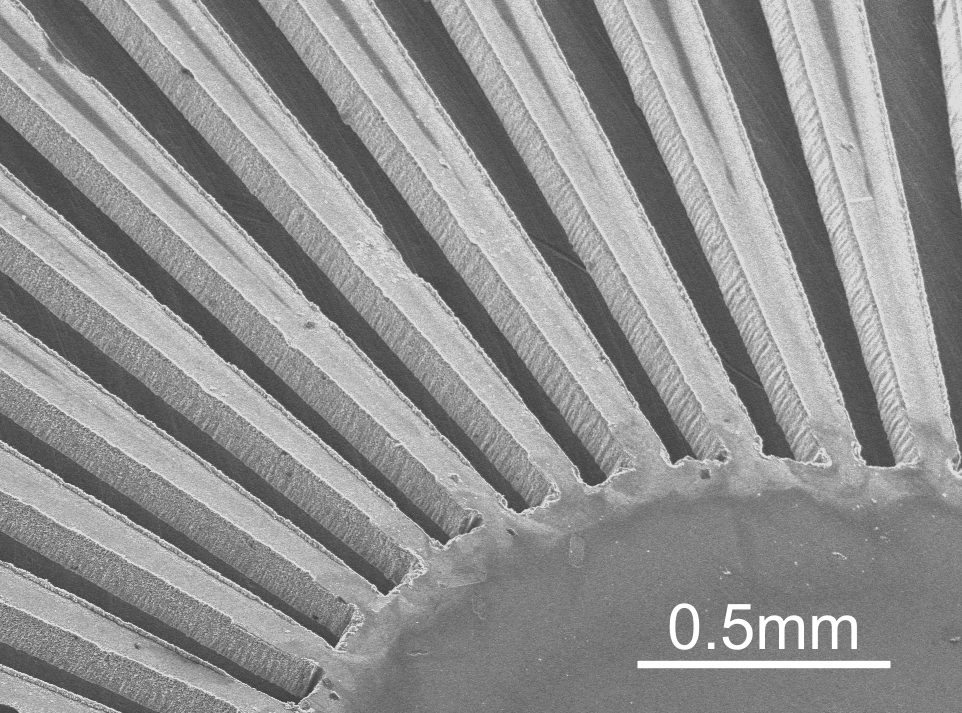
Laser ablation is a perfect toll for thin foil processing. High quality and accuracy is obtained during fabrication. It is possible to process various materials – metals, polymers, semiconductors, and ect. Part accuracy <5 µm can be obtained, while we can process foils up to 0.5 mm.

Multilayer thin-film processing is applied with ultrashort laser pulses. Low thermal damage of ultrashort laser pulses and selection of proper wavelength can significantly increase the thin-layer removal selectivity and quality. Our team has carried out several projects on thin-film P1, P2 and P3 patterning for CIGS, CZTSe, Silicon and organic solar cells. We have gained beneficial experience in this field and can offer process solutions for R&D and industry.

Laser induced periodic surface structures have found many applications during the last decade: control of surface wetting; friction reduction; colouring the surfaces; light absorption enhancement. We provide laser patterning with controllable period varying from 200 nm to 600 nm of various materials (metals, polymers, glass)

CONTACTS
MB “Šviesos Tankis”
Company code: 304837585
VAT: LT100012127017
Address: Savanorių pr. 235,
LT-02300, Vilnius, Lithuania
info@lightdensity.eu
+37060004346

